
74HC165 Shift Register
An 8-bit parallel-in, serial-out shift register used to expand digital inputs on a microcontroller.
Component Preview
The 74HC165 is an 8-bit parallel-in/serial-out shift register. It takes up to 8 individual digital inputs (like 8 buttons or switches) and allows a microcontroller to read all 8 states using only 3 digital pins. Multiple 74HC165 chips can be daisy-chained to read an almost unlimited number of inputs.
Overview
When you run out of input pins on an Arduino, the 74HC165 is the standard solution. By parallel-loading the inputs into the chip's internal memory and then serially shifting them out one bit at a time, you can massively expand your input capabilities.
Pin Reference
| Pin | Type | Description |
|---|---|---|
| VCC | power | Power supply (3V to 5V). |
| GND | power | Ground reference. |
| D0-D7 | input | 8 parallel digital inputs to be sampled (e.g., buttons, sensors). |
| PL | input | Parallel Load (SH/LD). Active LOW. When LOW, loads the states of D0-D7 into the shift register. When HIGH, data can be shifted. |
| CP | input | Serial Clock (CLK). On the rising edge, data shifts one position. |
| CE | input | Clock Enable. Active LOW. Usually tied to GND permanently. |
| Q7 | digital | Serial Output (QH). Outputs the final bit. Connect to the MCU to read data. |
| Q7_N | digital | Inverted Serial Output (QH'). Rarely used. |
| DS | input | Serial Input (SER). Used for cascading. Connect to Q7 of a preceding chip. |
Configurable Attributes
This component currently has no configurable attributes in the simulator.
Working Principle
- Load Phase: By pulling the Parallel Load (
PL) pinLOW, the chip takes a snapshot of the digital states currently on pinsD0throughD7and stores them internally. - Shift Phase: When
PLis broughtHIGH, the data is locked in. The first bit (D7) appears on theQ7pin. - Every time the Clock (
CP) pin goes fromLOWtoHIGH, all stored bits shift over by one position, allowing the microcontroller to read each bit sequentially from theQ7pin.
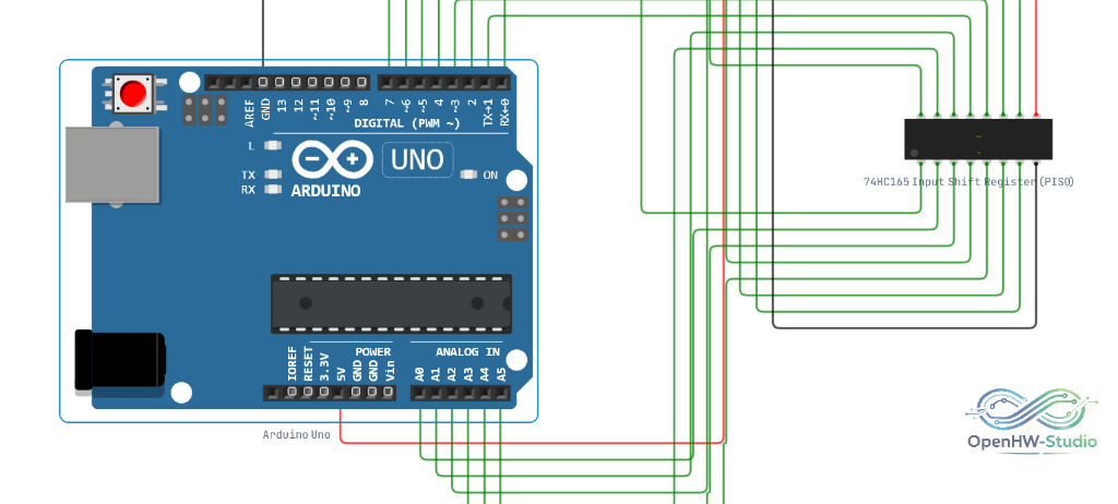
Wiring Diagram
Example of connecting a 74HC165 Shift Register to an Arduino Uno.
Example Arduino Code
const int plPin = 8;  // Parallel Load pin
const int cePin = 9;  // Clock Enable pin (can also just tie to GND)
const int q7Pin = 11; // Data Out pin
const int cpPin = 12; // Clock pin

void setup() {
  Serial.begin(9600);
  pinMode(plPin, OUTPUT);
  pinMode(cePin, OUTPUT);
  pinMode(cpPin, OUTPUT);
  pinMode(q7Pin, INPUT);

  // Initialize pins
  digitalWrite(cpPin, LOW);
  digitalWrite(plPin, HIGH);
}

void loop() {
  // Step 1: Sample the inputs by pulsing PL low
  digitalWrite(plPin, LOW);
  delayMicroseconds(5);
  digitalWrite(plPin, HIGH);

  // Step 2: Read the 8 bits from the shift register
  byte incomingData = shiftIn(q7Pin, cpPin, MSBFIRST);

  // Print the binary representation to the Serial Monitor
  Serial.print("Data: ");
  Serial.println(incomingData, BIN);

  delay(500);
}
Simulation Notes
- The simulator updates the output instantly upon clock edges and load commands.
- If you notice bouncing or inconsistent reads, verify that your virtual buttons have proper pull-up/pull-down configurations in your circuit layout.