
74HC595 Shift Register
An 8-bit serial-in, parallel-out shift register primarily used to massively expand the number of digital outputs on a microcontroller.
Component Preview
The 74HC595 is one of the most famous ICs in the maker community. It allows you to control 8 separate outputs (like LEDs, relays, or 7-segment displays) using just 3 pins on your microcontroller. Like the 165, multiple 595 chips can be daisy-chained together to control 16, 24, or even 100+ outputs from those same 3 pins.
Overview
Where the 74HC165 takes multiple inputs and collapses them into one serial line, the 74HC595 does the exact reverse: it takes a single serial line and expands it into 8 parallel outputs. It contains both a shift register (which receives data bit by bit) and a storage register (which holds the data steady on the output pins).
Pin Reference
| Pin | Type | Description |
|---|---|---|
| VCC | power | Power supply (3V to 5V). |
| GND | power | Ground reference. |
| Q0-Q7 | digital | The 8 parallel outputs. (Pins 15, and 1-7). |
| SER | input | Serial Input (DS). The pin where you send data bits one at a time. |
| SRCLK | input | Shift Register Clock (SHCP). Shifts data from SER into the internal memory on the rising edge. |
| RCLK | input | Storage Register Clock (STCP or Latch). Transfers data from the internal shift register to the output pins (Q0-Q7) on the rising edge. |
| SRCLR | input | Master Reclear (MR). Active LOW. Clears the shift register when tied to GND. Usually tied to VCC. |
| OE | input | Output Enable. Active LOW. Disables all outputs (high impedance) when HIGH. Usually tied to GND. |
| Q7S | digital | Serial Output. Used for daisy-chaining. Connect to the SER pin of the next 74HC595. |
Configurable Attributes
This component currently has no configurable attributes in the simulator.
Working Principle
- Shift Phase: You present a bit (HIGH or LOW) on the
SERpin and pulse theSRCLKpin HIGH then LOW. The bit enters the shift register. You repeat this 8 times for all 8 bits. - Latch Phase: Once all 8 bits are in the shift register, you pulse the
RCLK(Latch) pin HIGH then LOW. This copies the 8 bits simultaneously to the visible output pins (Q0-Q7). - Daisy Chaining: As you shift more than 8 bits into a single chip, the oldest bits "spill out" of the
Q7Spin. By connectingQ7Sto theSERpin of a second 595, the bits automatically flow into the second chip!
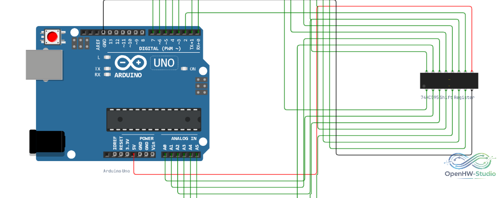
Wiring Diagram
Example of connecting a 74HC595 Shift Register to an Arduino Uno.
Example Arduino Code
The Arduino shiftOut function is designed specifically for this chip.
const int dataPin  = 11; // SER
const int clockPin = 12; // SRCLK
const int latchPin = 8;  // RCLK

void setup() {
  pinMode(dataPin, OUTPUT);
  pinMode(clockPin, OUTPUT);
  pinMode(latchPin, OUTPUT);
}

void loop() {
  // We will count from 0 to 255 and display it in binary on the outputs
  for (int i = 0; i < 256; i++) {
    // 1. Pull latch LOW to keep outputs steady while shifting
    digitalWrite(latchPin, LOW);

    // 2. Shift all 8 bits in
    shiftOut(dataPin, clockPin, MSBFIRST, i);

    // 3. Pull latch HIGH to push the bits to the outputs
    digitalWrite(latchPin, HIGH);

    delay(100);
  }
}
Simulation Notes
- The simulator visually represents the state of the internal registers and outputs instantly.
- If you cascade multiple 595s in the simulator, simply use
shiftOutmultiple times before pulling the latch pin high. (e.g., callshiftOuttwice to control 16 LEDs).